The world would be a very different place if the transistor had never been invented. They are everywhere. They underpin all digital technology, they are the workhorses of consumer electronics, and they can be bewilderingly small. For example, the latest Core i7 microchips from Intel have over two billion transistors packed onto them.
But what are they, and how do they work?
In some ways, they are beguilingly simple. Transistors are tiny switches: they can be on or off. When they are on, electric current can flow through them, but when they are off it can’t.
The most common way this is achieved is in a device called called a “field effect transistor”, or FET. It gets this name because a small electric field is used to change the device from its conducting ‘on’ state to it’s non-conducting ‘off’ state.
At the bottom of the transistor is the semiconductor substrate, which is usually made out of silicon. (This is why silicon is such a big deal in computing.) Silicon is a fantastic crystal, because by adding a few atoms of another type of element to its crystal, it can become positively or negatively charged. To explain why, we need to turn to chemistry! A silicon atom has 14 electrons in it, but ten of these are bound tightly to the atomic nucleus and are very difficult to move. The other four are much more loosely bound and are what determines how it bonds to other atoms.
When a silicon crystal forms, the four loose electrons from each atom form bonds with the electrons from nearby atoms, and the geometry of these bonds is what makes the regular crystal structure. However, it is possible to take out a small number of the silicon atoms and replace them with some other type of atom. If this is done with an atom like phosphorus or nitrogen which has five loose electrons, then four of them are used to make the chemical bonds and one is left over. This left-over electron is free to move around the crystal easily, and it gives the crystal an overall negative charge. In the physics language, the silicon has become “n-doped”.
But, if some silicon atoms are replaced by something like boron or aluminium which has only three loose electrons, the atom has to ‘borrow’ an extra electron from the rest of the crystal, meaning that this electron is ‘lost’ and the crystal becomes positively charged. This is called “p-doped”.
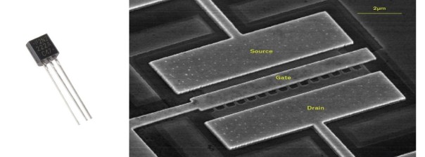
Okay, so much for the chemistry, now back to the transistor itself. Transistors have three connections to the outside world, which are usually called the source, drain, and gate. The source is the input for electric current, the drain is the output, and the gate is the control which determines if current can flow or not.
The source and drain both connect to a small area of n-doped silicon (i.e. they have extra electrons) which can provide or collect the electric current which will flow through the switch. The central part of the device, called the “channel” is p-doped which means that there are not enough electrons in it.
Now, here’s where the quantum mechanics comes in!
A while back, I described the band structure of a material. Essentially, it is a map of the quantum mechanical states of the material. If there are no states in a particular region, then electrons cannot go there. The “Fermi energy” is the energy at which states stop being filled. I’ve drawn a rough version of the band structure of the three regions in the diagram below. In the n-doped regions, the states made by the extra electrons are below the Fermi surface and so they are filled. But in the p-doped channel, the unfilled extra states are above the Fermi energy. This makes a barrier between the source and drain and stops electrons from moving between the two.

Now for the big trick. When a voltage is applied to the gate, it makes an electric field in the channel region. This extra energy that the electrons get because they are in this field has the effect of moving energy of the quantum states in the channel region to a different energy. This is shown on the right hand side of the band diagrams. Now, the extra states are moved below the Fermi energy, but the silicon can’t create more electrons so these unfilled states make a path through which the extra electrons in the source can move to the drain. This removes the barrier meaning that applying the electric field to the channel region opens up the device to carrying current.
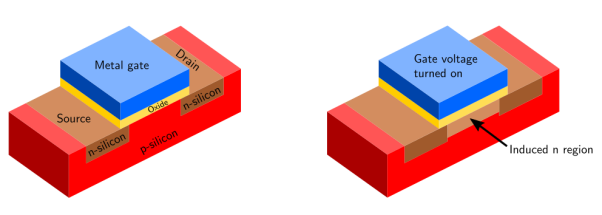
In the schematic of the device above, the left-hand sketch shows the transistor in the off state with no conducting channel in the p-doped region. The right-hand sketch shows the on-state, where the gate voltage has induced a conducting channel near the gate.
So, that’s how a transistor can turn on and off. But it’s a long leap from there to the integrated circuits that power your phone or laptop. Exactly how those microchips work is another subject, but briefly, the output from the drain of one transistor can be linked to the source or the gate of another one. This means that the state of a transistor can be used to control the state of another transistor. If they are put together in the right way, they can process information.
